This service is for you if:
- you have an electronic schematic and want to turn it into a professional PCB;
- you already have a prototype but are concerned about EMC or manufacturing issues;
- you need to prepare Gerber, ODB++, BOM files and production documentation;
- you want to reduce the risk of rework and delays;
- you need an external designer with expertise in PCB + electromagnetic compatibility.
- you have an idea for an electronic device (with clear specifications) and need full schematic + PCB design.
Not for you if:
- you need structured firmware development;
- you need to design FPGAs;
- you need to develop mechanical enclosures;
- you need to design high-voltage / high-current devices — flyback, PFC or power inverters.
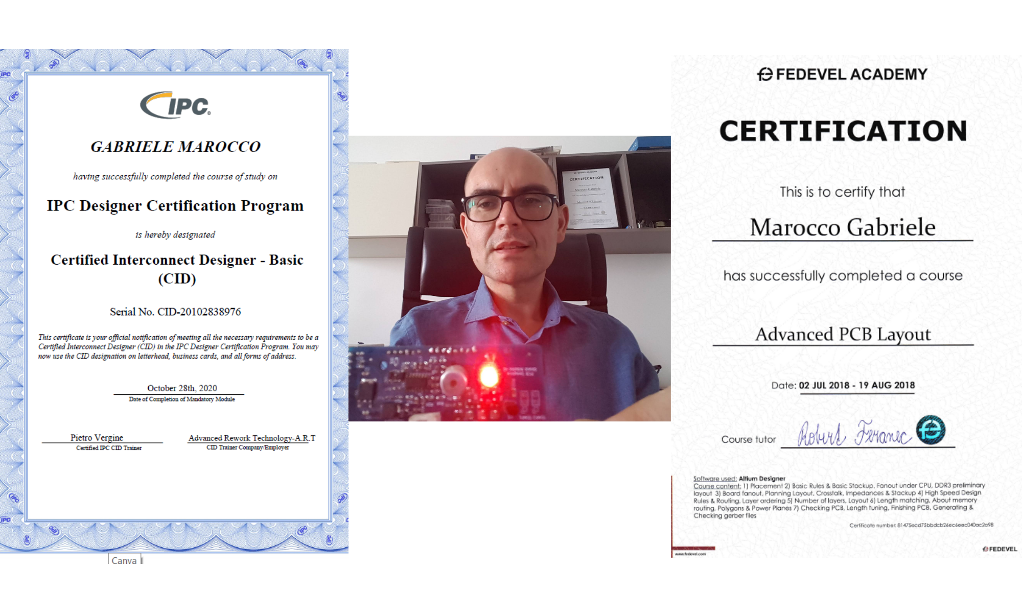
Gabriele Marocco
Electronic Circuit Designer
Professional Experience
For thirteen years I have been designing electronic circuits with a burning passion that drives every working day. This is not just my job — it is the engine of my technical creativity.
- Automotive
- Professional Drones
- Sensing & Sensors
- Home Automation Modules
Certifications
October 2020: IPC CID (Certified Interconnect Designer) certification
IPC is the organization that sets and regulates the design, manufacturing, and soldering standards for printed circuit boards, ensuring internationally recognised quality.
Software & Tools
I have worked with both professional and open-source PCB design software:
- KiCad (Preferred)
- Altium Designer
- Cadence (OrCAD)
Design Philosophy
"Today, when I create a printed circuit, I imagine a living organism. The traces are the veins and arteries, the signals are the vital impulse that flows silently but powerfully, and the vias are the essential communication points — like nerves transmitting vital information. The components are the organs, each with a unique and indispensable function."
But there is more: a circuit, just like a human body, lives in delicate equilibria. If a current flows in the wrong place, if an electromagnetic field interferes in the wrong way, the circuit suffers, loses efficiency, and cannot perform at its best.
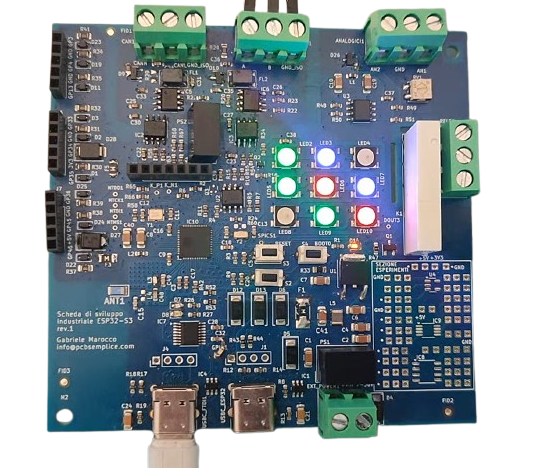
ESP32-S3 — Industrial Development Board
The challenge
Making an RF section and an isolated section dedicated to RS485 and CAN-BUS communication coexist on the same board, while preserving signal integrity across both domains.
GitHub Repository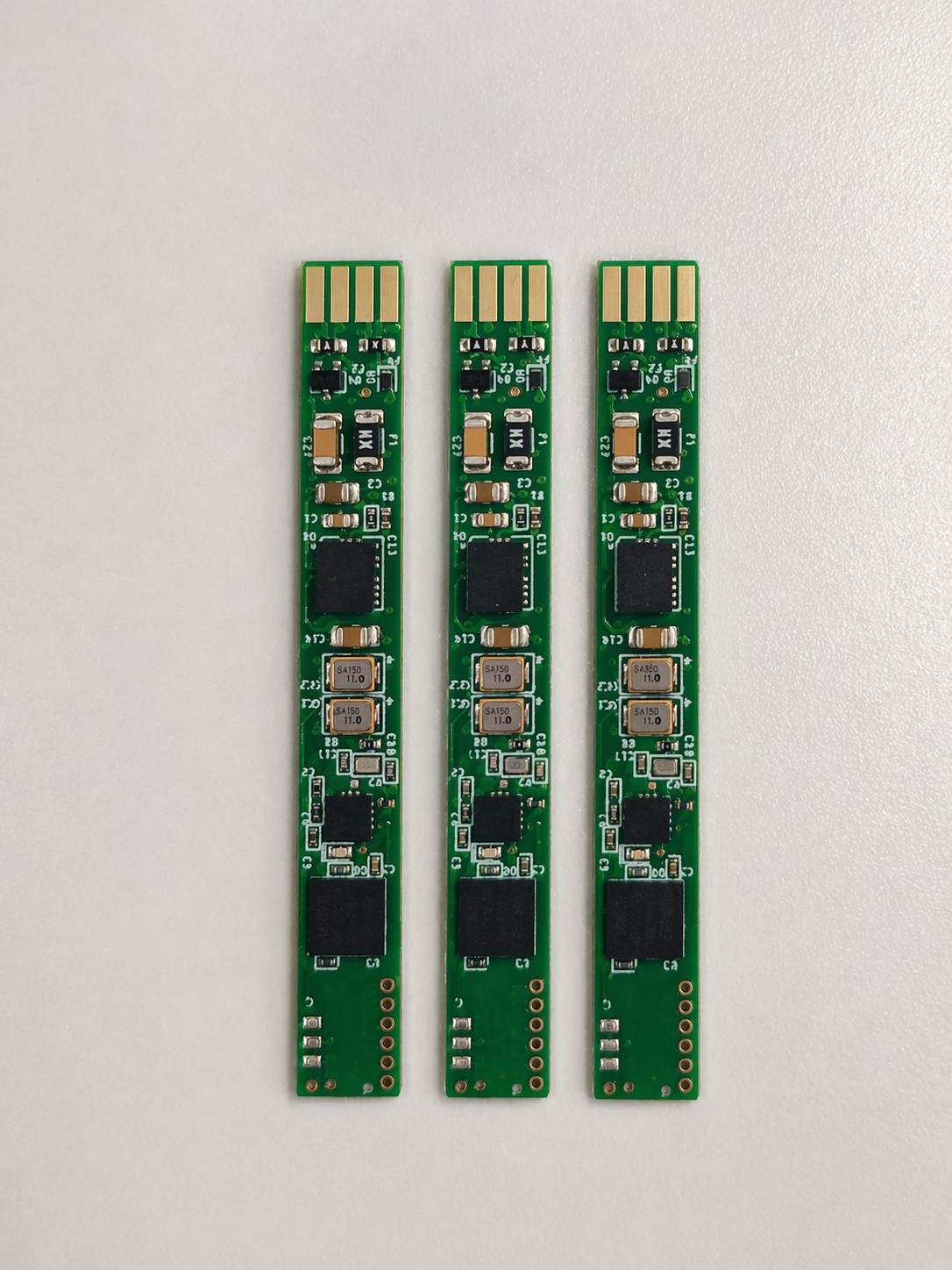
Industrial sensor
The challenge
The compact PCB footprint required using a BGA microcontroller with a 0.5 mm pitch, pushing the design into HDI (High Density Interconnect) territory.
Home automation module
The challenge
Finding a circuit solution and component placement that satisfied the enclosure constraints — while still passing EMC certification tests.
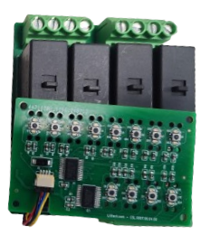
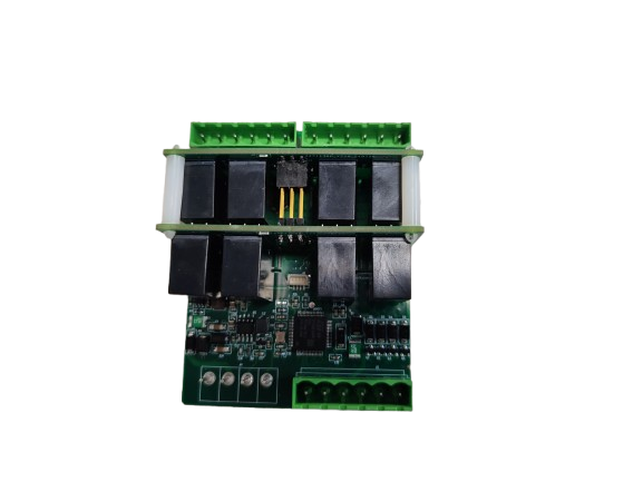
High-current home automation module
The challenge
Making low-voltage logic and the high-voltage / high-current power section coexist safely, with proper isolation — and passing EMC tests.
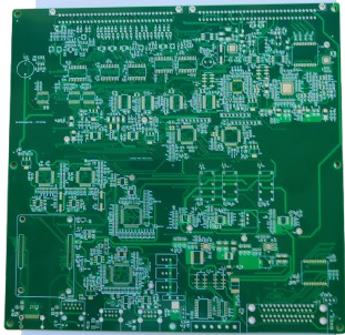
PCB for automated test bench
The challenge
Managing a high signal count while respecting the hard constraint of a maximum 4-layer stackup, optimising routing and domain separation throughout.