When you’re routing a circuit board, you need to know how much distance to keep between two tracks. What determines the minimum distance you have to keep?
![]() The first requirement that you have to meet is the minimum clearance required by the PCB manufacturer. This is typically 5 or 6 mils (0.127mm or 0.1524mm). Some manufacturers, with an extra cost, can make PCBs where the tracks are 4 mils (0.106mm) apart.
The first requirement that you have to meet is the minimum clearance required by the PCB manufacturer. This is typically 5 or 6 mils (0.127mm or 0.1524mm). Some manufacturers, with an extra cost, can make PCBs where the tracks are 4 mils (0.106mm) apart.
Pay attention that the minimum clearance required by the printed circuit board manufacturer also depends on the thickness of the copper layer: the greater the thickness of the copper, the greater the minimum space.
 The second requirement you have to consider is related to the voltage that flows in the track.
You must pay attention to this point when the voltage flowing in a trace is greater than 30Vac (alternating voltage) or 60Vdc (direct voltage). Regarding this point there are two terms that you find in the reference regulations.
– Clearance: is the minimum distance in the air between two conductors. Imagine that you have to measure the distance between two peaks of a mountain. The easiest way is to measure the distance in a straight line without following the outlines of the mountains. Returning to the conductors: if the minimum distance is not respected, conductive arcs can be created. You have also to consider that humidity and dust reduce the distance between two conductors.
– Creepage: is the minimum distance along the surface of the insulation material. This can be the distance between two traces in a PCB when there are no gaps. Indeed, in order to increase the creepage distance without growing PCB dimensions, in some cases you can design slots in the PCB

Where are defined the minimum spaces as a function of the voltage flowing between the conductors? They are defined in table 6-1 of the IPC2221B standard and in the IEC 60601-1 standard. The minimum spaces required are lower if the traces are in the internal layers of the PCB. For the traces in the TOP and Bottom layers the minimum spaces decrease if a protective varnish is applied (this process is also called conformal coating)
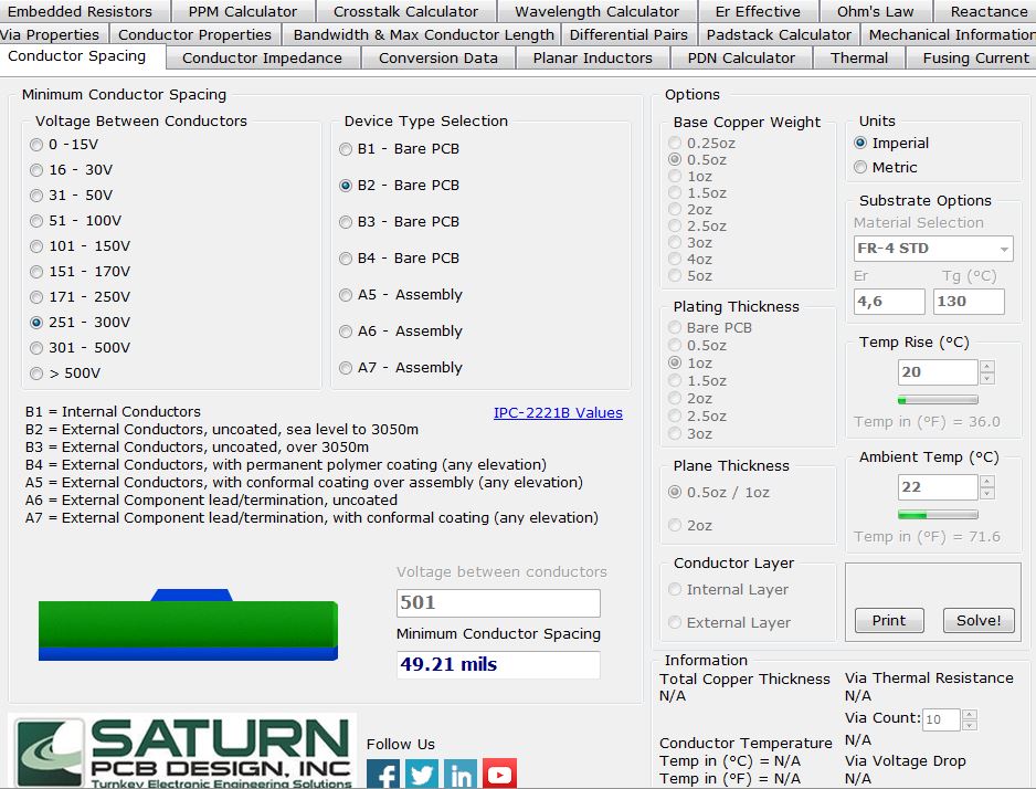
In order to detremine the minimum spaces it is not necessary to purchase the standards mentioned above. Indeed, there are free calculators. For example the SaturnPCB Toolkit software has a section called “Conductor Spacing”.
In the figure below the minimum space between two traces in the external layers has been calculated when the voltage is between 250 and 300V and no protective varnish is applied. In this case the traces have to be at least 49.21mils (1.25mm) apart from each other.
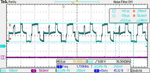
![]() If the voltages are less than 30V, the most important aspect to consider is crosstalk. In fact, an unwanted signal may be present in a track due to its proximity to another track. For example, a track in which a digital signal flows can generate an unwanted noise on the reset signal of a microcontroller.
If the voltages are less than 30V, the most important aspect to consider is crosstalk. In fact, an unwanted signal may be present in a track due to its proximity to another track. For example, a track in which a digital signal flows can generate an unwanted noise on the reset signal of a microcontroller.
For the reduction of crosstalk there are no reference standards but empirical rules (rules of thumb) based on simulations and measurements.
It is recommended to separate single tracks by a distance of 3W where W is the trace width.
When you have differential piar tracks it is recommended to keep a separation between two pairs of 5W.
Saturn PCB Toolkit software also helps you to estimate the crosstalk. In this case you can be satisfied when the values are below -30dB.
A final note. The crosstalk value depends also on the distance between the layer containing the track and the reference plane (this can be a ground or a power plane). This distance is often referred with the letter “h”. The smaller is this distance, the smaller is the crosstalk