Why do you have to take care of the temperature of your PCB(while it is working)?
 First of all because active electronic components (microcontrollers, memories, FPGAs, controllers for DC-DC converters) work correctly up to 85°C and in some cases up to 125°C. By this I am referring to the temperature indicated in the datasheets as Ta (it is the temperature of the environment in which the active component operates). Keep in mind that if your circuit board is placed in a metal box and there are parts that dissipate a lot of heat, sooner or later all this heat spreads throughout the PCB and as a result the “ambient” temperature will rise.
In addition to ambient temperature, another parameter to be considered for active components is the junction temperature Tj (junction temperature). The maximum junction temperature Tj typically varies between 125°C and 150°C. This parameter is specified in the section of the datasheet called “Absolute Maximim Ratings”
The “ambient” temperature and the maximum junction temperature are related by the formula
Tjmax=Ta+ Pd*Rth(j-a)
where Pd is the dissipation in W and Rth(j-a) is a coefficient that depends on the device package and on some layout tips (for example on how large is the copper area under the pad, on how many vias are placed under the pad).
Moreover. Consider that on extreme cases the track may catch fire or break.
OK, but what are the points to focus on in order to avoid overheating your circuit?
 Proper sizing of your PCB traces. There are several calculators (generally based on the IPC-2152 standard). One of these is the Saturn PCB Toolkit which in addition to provide the trace width for a given current, also gives an estimate of the temperature rise. When you deal with high currents, you can both increase the trace width and order a PCB with a thicker copper thickness. However, ordering a PCB with a thicker copper may involve an higher cost.

Proper sizing of vias diameter. The via current capability depends on its diameter and not on the anular ring size or on the via height. The same tools used to dimension the track width, estimate the via hole diameter. For example Saturn PCB Toolkit has a specific section focused on via properties.

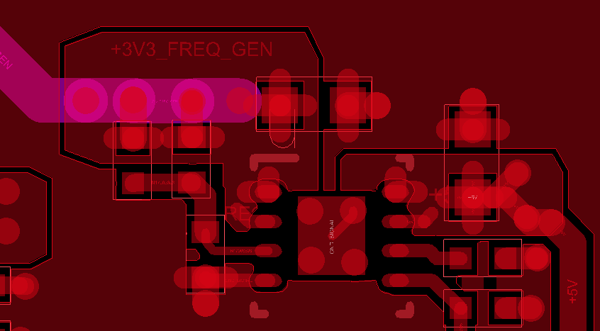
If the via diameter is too large, you can use multiple via holes. The figure below shows the layout of a linear regulator. The purple trace is connected to the polygon in the upper layer by three vias.
 Proper dissipation of linear voltage regulators, DC-DC converter modules and power transistors. For these components, pay close attention how you manage in the layout the largest pad of the component.
This pad (exposed pad) is connected either to the negative power supply reference or to the regulator output.
It is preferred to connect this pad with a polygon (or plane) rather than just with a track. On the basis of the width of the plane and the number of via holes present, the coefficient Rth(j-a) mentioned above changes. For example if you connect the pad with a small copper area, the coefficient may be quite high and therefore the dissipation capability is low. Instead, if you use a larger copper area Rth(j-a) deacreases
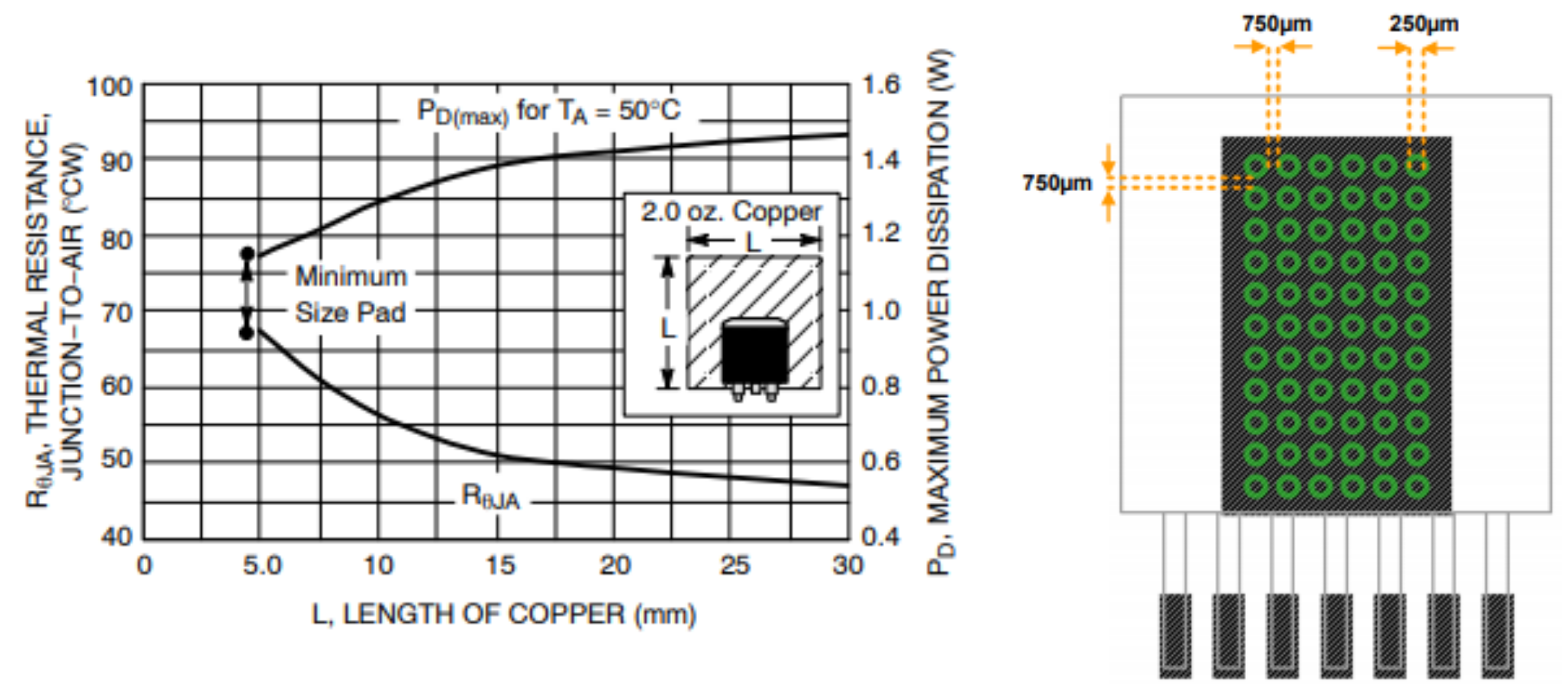
The image below on the left shows how the Rth(j-a) coefficient varies as a function of the copper area surrounding the central pad of the component.
The component referenced in the image is the voltage regulator NCP1117DT33T5G and the package is called DPAK. For this component the datasheet does not specify a pattern of via holes to be inserted inside the copper area.
The suggested pattern of via holes is shown in the picture on the right. In this case, the component is the step-down DC-DC converter controller 171012402 and its package is called TO263-7EP. In this case the exposed pad is located underneath the component body.
In multilayer PCB the presence of one ore more solid ground planes helps to dissipate the heat better.
A final note. In lighting or automotive application where heat dissipation is challenging, the structure of metal core PCB can be used. In this case the bottom or the internal copper layer is substituted with a metallic core. This layer has no tracks and act as a heatsink for the PCB. Metallic core PCB can be single layer, double sided PCB or multilayer

core