PCB layout design · No supplier lock-in
From your schematic to a PCB ready for production.And one you can maintain without me.
PCB design for companies that want to outsource layout without losing technical control of their project.
With the No Lock-in PCB Protocol™, I turn an established circuit schematic into a manufacturable, documented PCB that can be handed over to your team.
About 1 minute to complete · No obligation · Reply within 48 hours
Profile
Gabriele Marocco
Hardware and PCB designer · IPC CID since 2020

A real project
From a validated schematic to a working first prototype
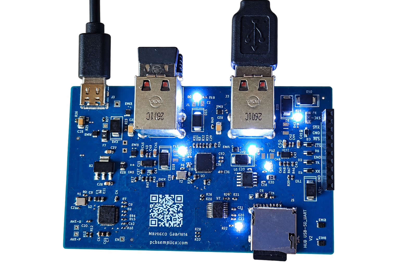
An electronic control unit for marine applications.
Read the full case study →The three weeks run from schematic validation to completed layout. No respin was needed in the checks described in the case study.
The problem after handover
Having the files does not mean you truly control the PCB.
You already have the schematic. The architecture is defined, the main components have been selected, and now you need a manufacturable board.
Outsourcing layout to a specialist is often the most efficient choice. The problem comes afterwards.
What happens if, six months from now, you need to replace a component, move a connector or change the PCB after testing?
If not, having Gerbers and source files is not enough. You may formally own the project while some of the know-how still lives in the original designer’s head.
Is this service a good fit for your project?
The service starts with an established circuit schematic. Every detail does not need to be perfect: the Readiness Gate, the initial review of requirements and design, is there to identify open issues before layout begins.
A good fit if
- You already have an established circuit schematic.
- The main components and circuit interfaces have been selected.
- Board dimensions and mechanical constraints are defined or close to final.
- You want to outsource layout while keeping source files and libraries under your company’s control.
- You want visibility into progress throughout the project.
- You want to approach the PCB manufacturer and electronics manufacturing services provider (EMS) with an organised technical package.
- You want future revisions to build on the existing design.
Not the right service if
- You only have an idea and still need to develop the electronic architecture.
- The schematic, main components and mechanical constraints are still changing constantly.
- You need to release the board for production within days by skipping the necessary technical checks.
- Your main priority is the lowest price for routing the traces.
Not sure whether your schematic is mature enough?
You do not have to decide alone. In the initial assessment, I review the available material and tell you whether we can start or what needs to be clarified before layout.
From a supplier-dependent project to a project under your control
| Typical traditional outsourcing | With the Protocol |
|---|---|
| Scattered decisions | Documented decisions |
| Production files | Source files + libraries + context |
| Updates on request | Tracked project status |
| Handover tied to one person | A transferable project |
A PCB should not depend on its original designer to keep evolving.
Case study
From requirements to working hardware, with no respin
Electronic control unit for industrial applications in the marine sector
Context
For this project, I also designed the circuit schematic, so the scope was broader than the service presented on this page. It included circuit development, PCB layout and technical support during production of the first prototypes.
The service described here starts from an established schematic. My circuit design experience helps me read that schematic and flag decisions that could affect the PCB before layout begins.
The problem: balancing isolation and cost
The inputs, outputs and communication signals needed to remain galvanically isolated from the microcontroller control section, while keeping the board’s cost under control.
I revised the architecture and schematics once to reconcile these requirements. For the input and output stages, I selected specialised ICs, considering robustness with long cables and electrically noisy environments, the interface to the microcontroller and component availability. This kept complexity, part count and sourcing risks under control.
Three key moments
Validate the schematic before layout
Before placement, I checked that the schematic captured the main requirements and that no open decisions remained that could affect the PCB. The review covered the entire design: the aim was to prevent an unresolved choice from becoming a late PCB change.
This is the check I now call the Readiness Gate: identifying incompatibilities and missing information while they are still inexpensive to fix, reducing the risk of later rework.
Plan placement and stack-up around isolation
I positioned the input and output stages to make good use of the available space while keeping the isolated sections separate. A four-layer stack-up, with the two inner layers providing continuous reference planes for the different sections, enabled controlled return paths and consistent separation between the isolated and control domains.
These choices reduced the risks of emissions and unwanted coupling. Placement and layout took approximately three weeks from schematic validation.
Support the project through to the EMS
I compared the costs and production capabilities of PCB and assembly suppliers and checked component availability in advance to limit late substitutions and manual work. During production, I handled technical discussions with the EMS, clarifying the mechanical specifications of some holes and checking several part numbers.
The result
The first prototype batch passed functional bring-up. At the stage of testing described here, the PCB had not required a respin. The project reached working hardware while keeping isolation, manufacturability and cost under control.
Feedback from the project coordinator
I worked with Gabriele on the PCB development of an industrial electronic control unit, in a project with several electrical, mechanical and manufacturing constraints.
I particularly appreciated his willingness to discuss technical issues, the care he put into the layout and his attention to the board’s manufacturability. The result was very positive: the first prototypes passed bring-up without any blocking issues related to the PCB.
It was a pleasant and constructive technical collaboration, and I would gladly involve him again in similar projects.
Five steps to keep control
The No Lock-in PCB Protocol™
Lock-in arises when part of the project stays outside the files. These five stages make the constraints, decisions and information needed to manufacture, modify and transfer the PCB explicit.
- 01
I remove hidden dependencies
Readiness Gate
Before layout, I clarify the schematic, components, constraints and information that would otherwise remain implicit.
Reduces dependence on: scattered information and undocumented decisions.
- 02
I make layout decisions understandable
Documented layout
I make critical constraints and decisions explicit, so anyone taking over the PCB can understand the reasoning.
Reduces dependence on: choices known only to the original PCB designer.
- 03
I preserve the context of decisions
Weekly updates
Each week, I record progress, decisions and open issues to keep the team aligned and the context available.
Reduces dependence on: memory and informal conversations.
- 04
I prepare the transition to production
DFM review and technical discussions with the EMS
I check the consistency of fabrication and assembly files and, where included, support technical discussions with the EMS.
Reduces dependence on: a single person for production clarifications.
- 05
I leave the project in your hands
Technical handover
I deliver the agreed source files, libraries and documentation so your team or another designer can pick up the work.
Reduces dependence on: the person who created the original layout.
More about the checks and technical handover
- Before layout
- I check the schematic, main components, mechanical constraints, connectors, interfaces, electrical requirements and production information. We address critical points before they become PCB rework.
- During layout
- I consider manufacturability and technical clarity, preserving the reasoning behind decisions that may affect later revisions.
- Throughout the project
- Updates cover completed work, relevant choices, issues and open points, including decisions that affect production and future revisions.
- Before production
- The manufacturing review prepares a consistent package for the EMS. Support with technical queries applies where included in the service.
- At handover
- You receive the agreed source files, libraries, production files and documentation of design decisions. A guided layout walkthrough is included where specified in the package.
The project stays with your company. You choose who works on it.
You can keep working with me, handle revisions internally or hand the work over to another designer.
About 1 minute to complete · No obligation · Reply within 48 hours
The handover in practice
What you receive
A technical package to manufacture the PCB today and work on it tomorrow, without rebuilding the context from scratch.
The contents are agreed according to the project and service level. The walkthrough, BOM review and EMS support apply where included in the package.
Complete project source files
You receive the PCB source files used during development. Your team or another professional can reopen and modify the project.
I work mainly with KiCad, an open-source CAD tool: your team can open and edit the source files without buying licences. If the project was started in Altium Designer or OrCAD, I can continue in that environment. Before starting, we agree on the format you need for the final handover.
Libraries used in the project
The footprints, symbols and necessary libraries accompany the design as agreed in the scope of work. A future revision should not stall because essential items were left on my workstation.
Fabrication and assembly package
You receive the files needed by the PCB manufacturer and EMS, prepared and checked before handover.
Files the package may include
- Gerbers or equivalent fabrication files.
- Drill and pick-and-place files.
- BOM and assembly data.
- Drawings, technical notes and additional files required by the manufacturer, as agreed.
Documentation of key decisions
I record electrical, mechanical and manufacturing constraints, along with the decisions made during development. Even months later, you can recover the reasoning behind a particular part of the layout.
Guided layout walkthrough
Where included in the service, a guided walkthrough explains the main PCB areas and the decisions you need to understand before making changes.
What the walkthrough may cover
- Critical sections, sensitive areas and specific constraints.
- Decisions related to fabrication or assembly.
- Points to keep in mind for future revisions.
A clear picture of the BOM
Where included in the package, I review the bill of materials to flag the main points that need attention before ordering. This check helps identify apparent issues and does not replace procurement.
What is checked
- Hard-to-source components and supply risks.
- Unclear part numbers or codes that need checking before ordering.
- Alternatives to evaluate.
Support for the handover to the EMS
If your company does not have an in-house PCB fabrication and assembly department, I support technical discussions with the EMS during the initial production or prototyping stages.
Queries I can help with
- Fabrication and assembly files.
- Components and PCB details.
Files, libraries, context and decisions stay together.
The value of the final package is technical continuity. When the project needs to be manufactured, modified or handed over to someone else, the work already completed remains the starting point.
The PCB remains usable as people, suppliers and requirements change.
About 1 minute to complete · No obligation · Reply within 48 hours
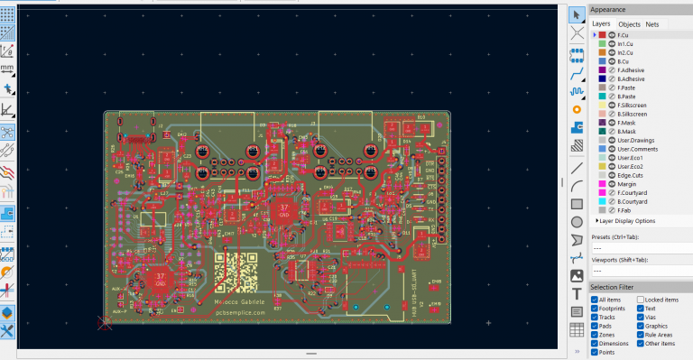
Two types of project
PCB complexity determines the work required.
Prices reflect the analysis, constraints and checks the board requires. Both options follow the No Lock-in PCB Protocol™.
Both options
You retain control of the project: the agreed source files, libraries and documentation to maintain and transfer the PCB.
Conventional PCB
PCB Continuity
- Standard components and a mature schematic.
- Clearly defined mechanical and electrical constraints.
- Established layout techniques, without HDI or challenging BGAs.
Work involved
Placement, routing and manufacturability checks for a project of limited complexity.
When it fits and what is included
For turning a mature schematic into a PCB ready for prototyping or production, with a design that can be modified, understood and transferred.
Typical project characteristics
- Defined architecture and mainly standard components.
- Clear mechanical constraints.
- A stack-up and layer count that are not particularly complex.
- No HDI or challenging fine-pitch BGAs.
- Electrical requirements that can be handled with established layout techniques.
- A bill of materials of limited complexity.
Included activities
The complete process described below: initial review, PCB design, manufacturability checks, updates, production files and technical handover.
PCB with greater technical challenges
PCB Continuity — Complex Projects
- BGAs, HDI or high component density.
- Challenging currents, voltages or thermal requirements.
- Sensitive signals, multiple PCBs or complex manufacturing constraints.
Work involved
Analysis of critical issues and management of interactions between electrical, mechanical and manufacturing constraints.
When it fits and what is included
For projects where a small change may affect several PCB sections, manufacturability or board behaviour.
Typical technical challenges
- BGAs or fine-pitch packages; HDI or microvias.
- High component density or multiple interconnected PCBs.
- High currents or voltages requiring particular attention to clearance and creepage.
- Tight mechanical constraints or thermal challenges.
- Sensitive signals or circuit sections; a more complex stack-up.
- Greater DFM risk or more involved coordination with the EMS.
Additional work based on the project
Includes the process common to both options. Additional activities are defined in the quotation and may include:
- More detailed technical analysis
- To identify critical issues and potential rework early.
- Advanced constraint management
- To account for interactions between electrical, mechanical and manufacturing requirements.
- In-depth DFM review
- To check the design before prototyping or production.
- BOM Health Check
- To highlight components and BOM items that need checking before ordering.
- Technical layout walkthrough
- To transfer the context of key decisions to your team.
- Support in discussions with the EMS
- To handle technical queries during the transition to production.
The final quotation depends on complexity, layer count, components, mechanical constraints and electrical requirements. The scope of work is agreed for your project.
Prices cover PCB design and engineering. Physical board fabrication, components and assembly are excluded.
Activities included in both options
Readiness Gate
Initial review of the material and constraints before layout.
PCB design
Placement, routing and layout development to meet the requirements.
Manufacturability checks
PCB checks before generating the final files.
Project traceability
Updates and records of key technical points.
Production package
Files needed for fabrication and assembly.
No Lock-in Handover™
The agreed source files, libraries and technical material needed to resume work on the design.
You do not have to choose a package on your own.
The initial assessment clarifies how mature the schematic is, its constraints and the level of analysis needed. I recommend the appropriate option: if the PCB does not need a higher level of analysis, there is no reason to treat it as if it does.
About 1 minute to complete · No obligation · Reply within 48 hours
Guarantees
Clear commitments before we start.
It would not be realistic to promise that a PCB project will never encounter issues, revisions or technical challenges.
My guarantees cover how I manage your project, the deliverables you receive, and the information that remains under your company’s control.
Complete Handover Guarantee
At handover, you receive all agreed deliverables: source files, libraries, production files and the documentation included in the service.
If your team or EMS identifies a missing agreed deliverable within 30 days of handover, I will provide it at no additional cost.
In practiceThe project is not closed until the agreed package is complete.
Project Continuity Guarantee
I organise the agreed files and materials so the project can be archived, reopened and handed over to your company or another professional.
I cannot guarantee that a new designer will agree with every design decision. I can guarantee they will not have to start with an incomplete folder or rely on files stored only on my computer.
In practiceIf you continue with someone else tomorrow, the project remains yours.
Clarity Before Layout Guarantee
Layout does not begin until the key constraints are sufficiently clear.
If the Readiness Gate reveals an issue that makes it too early to start, I flag it before design work begins.
In practiceBetter to pause a day earlier than discover weeks later that a key decision is missing.
The earlier you check the constraints, the less corrections cost.
If your schematic is close to final, this is the right time to check the feasibility of the layout.
The most expensive problems are those discovered after the mechanics and components have already been frozen.
Let’s see whether your schematic is ready to become a PCB.
Request a free initial project assessment. Before we start, I assess the maturity of the schematic, the complexity of the layout and the most suitable service option.
How does the service work?
- 01
Complete the form below
In the text field, please specify whether this is a straightforward project or a more complex project. I prefer to use KiCad, but I can also work with Altium Designer or Cadence if you already have draft designs in those CAD tools.
- 02
Reply within 48 hours
- 03
Online meeting
If you would like, we can arrange an online meeting to get to know each other and discuss the project.
- 04
Non-disclosure agreement (NDA) and service contract
You will receive a signed non-disclosure agreement covering the information you provide, together with the contract setting out the service terms and conditions.
- 05
Payment and delivery
Before starting, I will ask for a 50% deposit on the quoted amount.
The balance will be due within 30 days of delivery of the final technical documentation.
Support during prototyping and production is provided as technical coordination, not as the direct supply of assembled PCBs.
Emissions control belongs in the layout, not at the end of the project
An EMC issue found during certification means a PCB change on a board that has already been manufactured. The cost is not just the new revision: it is the weeks of delay and the prototype batch that has to be rebuilt.
This is why I completed a 1:1 training program on electromagnetic interference control with Dario Fresu, an EMI/EMC specialist. The practices that came out of it are part of how I set up every layout today, from stack-up selection to the handling of return paths.
Gabriele completed our 1:1 EMI Training program with dedication and a strong willingness to learn. From the start, he showed a solid understanding of EMI challenges and quickly applied best practices to his circuit designs. His ability to grasp complex concepts and implement them effectively was impressive.
Beyond his technical skills, Gabriele's curiosity and proactive approach made working with him a great experience. He made insightful questions, engaged deeply with the material, and showed a genuine commitment to mastering EMI mitigation. His strong work ethic and attention to detail set him apart.
I highly recommend Gabriele to any team or project that values strong EMI control and high-quality circuit design.
Gabriele Marocco PCB Designer, IPC CID
I have personally taken 10 boards into production: 9 home automation modules and 1 industrial vibration sensor.
- 10boards taken into production
- 9/9home automation modules: EMC passed on the first attempt
- 12+years working on electronic circuits
All 9 home automation modules passed EMC testing on the first attempt. The vibration sensor needed a single fix — changing the value of two capacitors to pass conducted RF immunity — which I identified and closed out without redoing the layout.
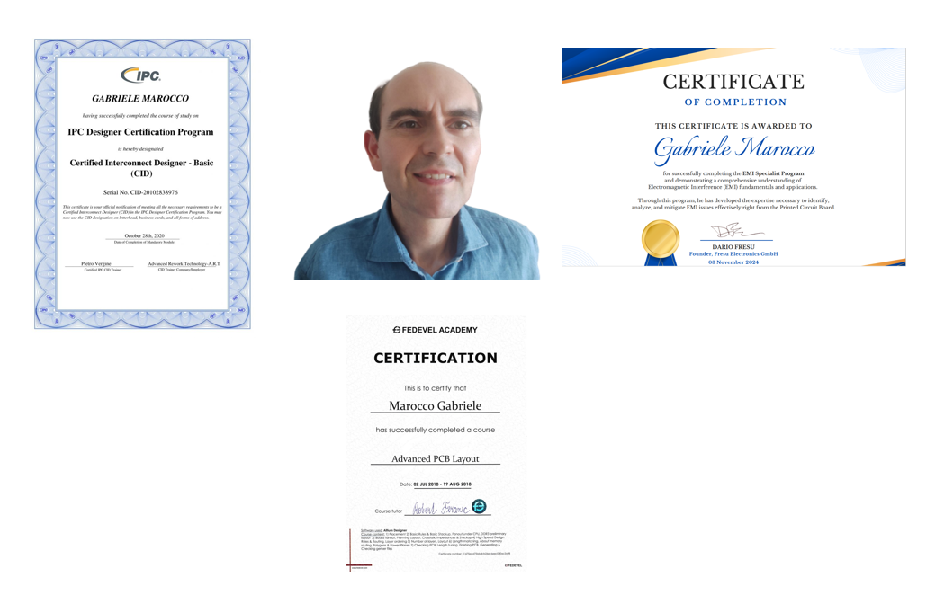
I mention that last case on purpose. An immunity test never lets a rough choice : the gap between "passes first time" and "weeks of respin" can come down to two capacitors decided during layout. That's why I work on the details before the board reaches the lab, when fixing them costs an hour instead of a board revision.
I work mainly with KiCad, with open source files owned by the client. IPC CID (Certified Interconnect Designer) certified since 2020, over 12 years on electronic circuits, the last 3 focused on home automation and industrial sensing — the sectors where EMC and field reliability are not negotiable.
I work under the No Lock-in PCB Protocol
- Every week you receive a report or an update call
- The project files are yours
- The components I select are easy to source
Here are some boards I've designed
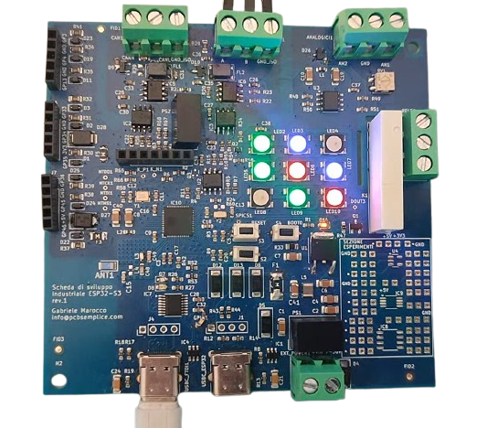
ESP32-S3 — Industrial Development Board
The challenge
Making a radio-frequency section coexist with an isolated section dedicated to RS485 and CAN-BUS communication, while maintaining signal integrity in both domains.
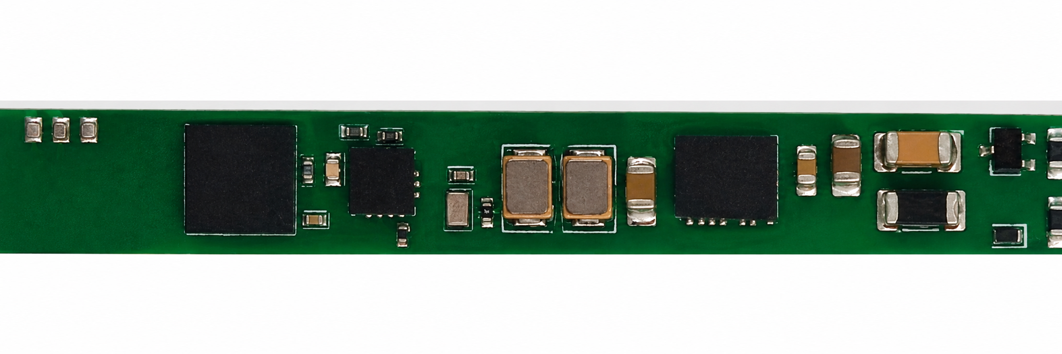
Industrial sensor
The challenge
The small PCB dimensions required the use of a BGA microcontroller with a 0.5 mm pitch, taking the project into HDI (High Density Interconnect) territory.
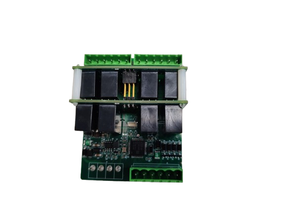
Home-automation module
The challenge
Finding a circuit solution and a component layout able to respect the constraints imposed by the enclosure, while ensuring the EMC tests are passed.
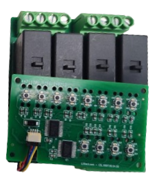
High-current home-automation module
The challenge
Making the low-voltage logic coexist with the high-voltage, high-current power section, ensuring proper isolation and passing the EMC tests.
PCB design services — FAQ
What exactly does a PCB layout designer do?
A PCB layout designer takes an established circuit schematic and turns it into a manufacturable, documented design that can be maintained over time. In practice, this involves checking mechanical and circuit constraints, placing components, routing the board, running DRC/DFM checks and preparing the files needed by the PCB manufacturer and EMS.
It is more than drawing traces. The designer’s role is to turn a schematic into a technical package that your company can manufacture, test, modify and maintain after handover, without being tied to the person who did the work.
Do you also manufacture and assemble the physical PCB?
No. This is a PCB engineering service: technical design review, layout, documentation, production files and technical coordination with the PCB manufacturer and/or assembler. Physical board fabrication, component purchasing and assembly are not included, except under separate agreements with the suppliers involved.
If requested, I can support the start of production with the manufacturer or EMS by uploading files, answering technical queries and checking that the delivered package matches production requirements. My role remains the project’s technical point of contact, rather than a reseller of the physical boards.
What information do you need for a reliable quotation?
An up-to-date schematic, BOM, mechanical constraints, intended production target, any EMC notes or critical requirements, the CAD tool already used internally and the project’s current maturity. Clearer starting material leads to a more realistic quotation and less scope for rework.
What is included in the service?
The service generally includes the initial readiness check, stack-up planning, component placement, PCB routing, DRC/DFM checks, preparation of design and production files, delivery of the annotated BOM and technical coordination with the manufacturer/EMS, as defined in the quotation.
What is not included?
PCB fabrication, component purchasing, assembly, laboratory costs, product certification, regulatory testing, firmware and schematic changes outside the agreed scope are not included. Requests outside the project scope are handled as additional work.
What deliverables will I receive?
A typical handover includes editable project source files, the libraries used or needed for maintenance, PCB fabrication and assembly files, the agreed technical documentation, the BOM with any relevant notes, and a STEP 3D model where included. If agreed, the package can also include ODB++ or other formats useful to the manufacturer’s or EMS’s workflow.
The aim is to deliver more than Gerbers and pick-and-place files: you receive an organised package that your team or another supplier can reopen and manage. This is central to avoiding technical lock-in and having to start from scratch at the first revision.
Do you also work with the PCB manufacturer or EMS?
Yes, this can be part of the service. If you do not already have a preferred supplier, I can support the selection of a suitable manufacturing route, upload files to supplier portals, check the consistency of the technical package and answer practical queries from the factory or assembler.
If your purchasing department or engineering team already has a supplier, my role is to act as the technical interface: clarify data, add any missing files included in the scope and help avoid misunderstandings between design and production.
Who chooses the manufacturer or assembler?
You can choose the supplier yourself or ask me for technical support in selecting a suitable option. The final commercial decision remains with your company unless we agree otherwise.
Who is responsible for circuit design decisions and product requirements?
Responsibilities need to be clear from the start. The PCB layout designer takes responsibility for the layout, consistency of the technical package and the interface with production for matters arising from the layout itself. Electronic architecture, functional requirements, system performance, firmware and final product validation remain the responsibility of the client or circuit designer, unless agreed otherwise.
This distinction is intended to prevent incorrect expectations. A good layout reduces risk and rework, but it cannot replace properly defined requirements or system validation.
Who owns the files, source files and intellectual property?
Unless agreed otherwise, the design and documentation developed for your project belong to your company.
Can we sign an NDA before sharing files?
Yes. This is a normal and recommended request when sharing schematics, BOMs, mechanical constraints or product documentation. The NDA can be signed before technical material is shared and before the final quotation is issued.
What does “no lock-in” actually mean?
It means that at handover you receive not only the files needed for manufacturing, but also the files needed to understand, reopen, modify and maintain the design. If you later need to change a component, update the enclosure or move to another EMS, you do not have to start from scratch.
Will the design remain reusable if we change PCB supplier or EMS?
This is one of the service’s main objectives. The package is prepared to reduce dependence on a single supplier and support technical continuity over time.
Will I receive an invoice for the service?
Yes. A formal electronic invoice is issued for each stage specified in the quotation.
The project normally starts after payment of the initial deposit stated in the quotation. The balance is due on the agreed terms, generally within 30 days of delivery of the final technical documentation.
These invoices are not pro forma documents: they are tax documents submitted through Italy’s Sistema di Interscambio (SdI). Payment must therefore be made by the due date shown on the invoice.
What happens if errors are found when the board arrives?
A complex electronic board may require checks, testing and sometimes a revision after the first prototype. That is why the service includes technical support during prototyping and production, as agreed in the quotation.
If an error is attributable to the files I delivered or to work I performed within the agreed scope, I will correct the necessary files free of charge and, where possible, propose technical solutions to recover boards already manufactured or reduce the impact of rework.
This does not cover errors arising from circuit design decisions outside my assignment, incomplete requirements or requirements changed after approval, firmware issues, assembly errors, unapproved component substitutions, manufacturer/assembler limitations or decisions taken by the client without my technical review.
Handling an error or revision does not justify withholding payment of invoices for work already completed and delivered, unless otherwise agreed in writing.